

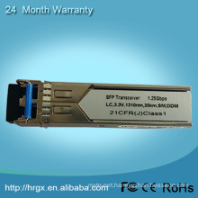
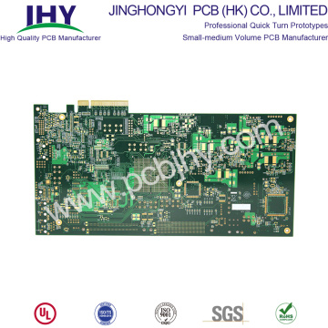
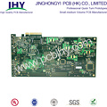
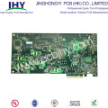
Circuit Board Gold Fingers
Product Description
Circuit Board Gold Fingers
In the realm of PCB assembly and manufacturing, there are three different methods that come with printing the prototype PCB`s legend. The legend is what the engineer uses to figure out the component designators, switch settings, and test points - all helpful components need when assembling, testing, and servicing the prototype circuit boards.
However, there are more details that go into this legend, including gold plating. Here is a beginner`s guide to this specific PCB fabrication process.

Gold finger is the gold-plated connectors that are on the edges of the printed circuit board prototype. They are similar to fingers in that they are long and narrow.
What are Circuit Board Gold Fingers made from?
The specifications for these have to be exact; flash gold must be used and the thickness cannot go over 3Us to 50Us. This is so the flash gold, which is one of the hardest golds available, will last a long amount of time and won`t need repair.
What is Circuit Board Gold Fingers purpose?
Gold fingers are edge connector contacts and are used to electroplate pads onto the board. The idea behind a gold finger is to help protect the printed circuit board prototypes from wear and tear. If applied correctly, with the right thickness, they are expected to last upwards of 1,000 cycles before there is any need of repair.
How are Circuit Board Gold Fingers used?
These little fingers are quite versatile, and they have many different uses depending on their intended purpose. Some of these uses include:
- Provides connections for network transfer data.
- Attaches specialty adaptors.
- Connects different devices to the board.
- Can be used as audio adaptors.
- Are there specific design specifications?
Yes. As we mentioned previously, there are some specifications depending on the need and use of the board. However, despite this, there are some design rules that must be followed no matter the board`s intended purpose. This includes:
- No plated through holes can be included anywhere near the gold fingers.
- No soldermask or screen printing can be included near the gold fingers.
- The gold fingers should always be placed facing outward of the board`s center.
Circuit Board Gold Fingers manufacturing service


The attributes of the displayed product
Type Gold Fingers PCB Layers 8L Base Material FR4 Tg170 Dielectric Prepreg Board Thickness 1.6mm±10% Copper Weight 1oz Surface Finish ENIG 2U"+Gold Plating 45U" Minimum trace Width/Spacing 0.13/0.13mm(5/5mils) Solder Mask Color Green Silkscreen Color White Min. Hole Size 0.15mm Hole Copper Wall Thickness 25.4um Flame Retardant Properties 94 V-0 Application Industrial Controllers
Why choose us?
- Save money&time! Achieve peace of mind!
- A professional and trustworthy PCB prototype manufacturer.
- Fastest PCB Prototype.
- One stop solution for various PCB&SMT Stencil.
- Low cost for simple PCB.
- Affordable price for high-tech PCB.
- Minimum orders 1pcs.
- 24-hour online customer service.
- Professional PCB engineer for one-to-one service.
- Shipment on time.
- Guarantee good service and quality from PCB quotation to delivery.
Certification(UL:E466618, TS16949, ISO9001.RoHS)
Quality is one of the cornerstones in Global Success' business. We work actively with continuously improvements to secure a high quality level on our products as well as our services. To satisfy our customers we focus on producing PCB with stable top quality. We have implemented the UL:E466618, TS16949, ISO9001.RoHS quality system. The perfect quality assurance system and with various inspection equipment`s help us to monitor the whole production process, assure stability of this process and high product quality, meanwhile, advanced instruments and technology methods have been introduced to attain sustained improvement.
 |  |  |
Electronics Fair
We took part in the famous exhibitions (As a PCB manufacturer) over the past years and got high appreciation from the top experts and customers, as well as cooperated tightly with them.

PCB Shipment
JHY PCB offers flexible shipping methods for our customers, you may choose from one of the methods below.

Shipping Process
After production and testing, your PCB orders will be sent to our shipping department. As the Gold Fingers PCB manufacturer, JHY PCB shipping department will ship your PCB quickly without any pending.
JHY PCB 's Packing Way
- Use one professional PCB vacuum bag, with desiccant inside. Vacuum compressed totally.
- Paste label and RoHs mark. Use second vacuum bag to protect boards again, vacuum compressed, make sure no exception.
- Microsection report and Tin testing board are put together with PCB in cartons.COC (Certificate of Conformity) will be sent to customer by email in PDF.
- Several layers of thick EPE(Expand aple poly ephylene) are filled fully in gaps between PCBs and cartons. Thickness of 1 layer EPE is 10mm.
- Neutral Packing is adopted if no special requirements. Strong and thick cartons(Thickness:10mm,7 layers). Different sizes of cartons are designed to meet demand of different PCB size. All package are within weight limit of cartons. For mass production order, no exceed 21kg per carton normally.
- All cartons sealed with strong adhesive tape should be sealed twice so as to make them more durable.
- Solid PP/PET strapping is used outside of cartons.
- Shipping mark, fragile mark and postcode label are all pasted clearly.
How to ship your PCB?
- Firstly, JHY PCB shipping department will print order address and invoice.
- Secondly, JHY PCB will set the shipment information on the Logistics company website.
- Thirdly, the Logistics company staff will collect the package from JHY PCB and ship it to you.
Shipment Term
With the purpose of better customer service and meeting the customer demand, JHY PCB provides following shipping methods.
JHY PCB is experienced in exporting. For PCB Prototype and small-medium volume PCB order, we have stable and long-term good relationship with forwarder, such as international express company DHL, FedEx, TNT, UPS. For mass production order, we have famous and reliable shipping company for support.
FAQ
Q1: What is your minimum order quantity?
A: Our MOQ is 1 PCS.
Q2: Do you accept PCB design with different boards on one panel?
A: Of course, we can do different boards on the same panel.
Q3. Are my Gerber Files safe?
A: We protect the intellectual property for customers in the whole process. All documents from customers are never shared with any third parties.
Q4: What is needed for quotation?
A: Quantity, PCB Gerber file, Technical requirements(material, board thickness, surface finish, copper thickness, solder mask color, silkscreen color, ...)
Q5. How to quote shipping cost?
A: The shipping cost is determined by the shipment way(forwarder name, delivery days), destination, weight&dimension of packages. If you use your own forwarder, please inform us.
Product Categories : Gold Fingers PCB